FMG01/SCD/5
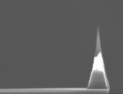
Single crystal diamond (SCD) cantilevers FMG01/SCD consist of standard silicon chips and consoles and high aspect ratio single crystal diamond needle grown in CVD process and fixed on a lever. Tip's cone angle of such AFM probes is less than 10 degrees. With such dimensions a tip may get into all deep trenches and gaps between particles providing impressive and detailed images. Having a competitive price on market SCD AFM cantilevers offer several noticable advantages to AFM researchers:
 Full diamond tip is harder than a standard silicone one. Its wear is about 10 times lower and it allows to measure surfaces that grind fast silicon needles. More of all, such cantilevers will be the best for measurements of surface elasticity properties. Their deformation during force curves processing will be minimal respectively to other-material tips;
- Tip's high aspect ratio (small cone angle) allows SCD cantilevers to get detailed images of objects with narrow walls;
- Low surface energy of diamond makes SCD cantilevers to be well-usable for long time scanning of sticky biological samples;
- Narrow and hard tips are also suitable for simple nanoindentation experiments with standard AFM parts.
Great utility of SCD AFM cantilevers for precise measurements is accompanied by a detailed quality control. After gluing a tip to a lever each cantilever is being observed by SEM before shipment. Thus only good probes reach the customers.
|
Calibrated SEM photo of tip's end
|
 On the image to the left the one may see calibrated SEM images of single crystal diamond tip's end.
 On the image to the right the one may find topography of so-called "Black silicon" relief obtained by a single crystal diamond probe. This surface consists of Si pyramids created by a special etching. It is characterized by very low reflectivity and is used in solar cells.
The main challenge of imaging such pyramides is their extreme height: 6-7 um. Only a very narrow and high tip could get between neighbour pyramides and show detailed topography of such sample. As it may be noticed from the image, our application scientist succeeded to get a high-quality scans with clearly visible side walls and other dimensions. Such image is impossible to get with standard cantilevers of 20-40 degrees cone angle.
Chip thickness H: 0,3mm.
Reflective side coating: Au.
Tip's cone angle: < 10 degrees.
Tip's aspect ratio: > 1:5.
Tip's curvature radius: < 10 nm.
Chip has one rectangular spring.
FMG01/SCD - for noncontact mode.
|
|
Cantilever length, L±5µm
|
Cantilever width, W±3µm
|
Cantilever thickness, µm
|
Resonant frequency, kHz
|
Force constant, N/m
|
SCD tip length, µm
|
|
min
|
typical
|
max
|
min
|
typical
|
max
|
min
|
typical
|
max
|
min
|
typical
|
max
|
|
noncontact
|
225
|
32
|
2.0
|
2.5
|
3.0
|
40
|
60
|
96
|
1
|
3
|
5
|
12
|
14
|
16
|
At customer's requirement tip side of the probes can be coated by conductive coating.
Other cantilever specifications are available. Please, contact us for more information.


 Full diamond tip is harder than a standard silicone one. Its wear is about 10 times lower and it allows to measure surfaces that grind fast silicon needles. More of all, such cantilevers will be the best for measurements of surface elasticity properties. Their deformation during force curves processing will be minimal respectively to other-material tips;
 On the image to the left the one may see calibrated SEM images of single crystal diamond tip's end.
 On the image to the right the one may find topography of so-called "Black silicon" relief obtained by a single crystal diamond probe. This surface consists of Si pyramids created by a special etching. It is characterized by very low reflectivity and is used in solar cells.