NT-MDT Spectrum Instruments – research, production, sales and support  of wide range AFMs and AFM-Raman-Nano-IR Systems


Ireland
Choose another
  
Shopping cart

Products

Excellent and Reliable TERS Cantilever-type Probes
 
 
The main advantages:
 
– Enhancement factors: 100x and more
– Lateral resolution in TERS: down to 10nm
– High speed TERS mapping
– Top-down illumination configuration (opaque samples)
– Based on commercial AFM cantilevers VIT_P series (contact, non-contact), multiple AFM modes, excellent imaging performance.
 
 
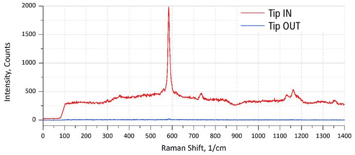
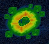
Fig. 1 Typical Raman signal enhancement (>100x) of NT-MDT Spectrum Instruments TERS AFM probe.
 
 
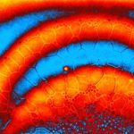
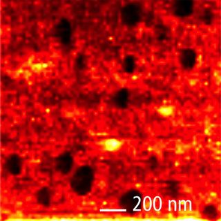
Fig. 2  High resolution TERS map. Resolution: ~20 nm.
Sample: BCB thin molecular layer on Au substrate.
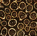
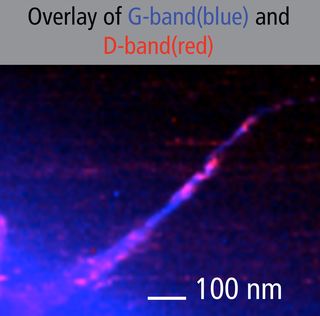
Fig. 3 High resolution TERS map of carbon nanotubes on Au substrate. Resolution: ~10 nm


TERS (nano-Raman) imaging by NT-MDT S I AFM-Raman instrument.
 
NT-MDT Spectrum Instruments develops and supplies unique instrumentation for AFM integration with various optical microscopy and spectroscopy techniques. NT-MDT Spectrum Instruments was the first to introduce an integrated AFM-Raman instrument in 1998 and is now the leading developer and supplier of such instruments worldwide.
NT-MDT Spectrum Instruments AFM-Raman instrument has been successfully used for TERS (nano-Raman) mapping of various objects with spatial resolution reaching 10 nm: graphene and other carbon nanomaterials, polymers, thin molecular layers (including monolayers), semiconductor nanostructures, lipid membranes, various protein structures, DNA molecules etc. References to corresponding publications can be found at www.ntmdt.com/afm-raman .
 
TERS probe challenge.
 
While the AFM-Raman instrumentation has been developing relatively fast, TERS probes have always remained the main limiting factor for nano-Raman to become a routine characterization technique.
The main challenges are:
- manufacturing reproducible probes with high enhancement factors and high resolution imaging capabilities;
- probe lifetime;
- probe ease of use;
- probe mass production not involving complicated and poorly reproducible manual procedures.
TERS probes originally used in scientific publications were usually etched metal wires - attached to tuning fork or working in STM (tunneling) regime. Preparation of such probes requires elaborate manual operations; probes are typically not very reproducible. Another approach to TERS probe preparation utilizes focused ion beam to manufacture special structure on the tip end. This approach is very resource consuming and also lacks reproducibility. Different metal coatings of AFM cantilevers have been reported recently – with different degrees of enhancements and reproducibility.
 
Reproducible TERS probes from NT-MDT S I.
 
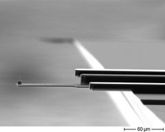
As a result of comprehensive research performed together with NT-MDT Spectrum Instruments customers and partners, NT-MDT Spectrum Instruments is now able to offer to its AFM-Raman customers mass produced reproducible cantilever-type TERS probes. The probes are prepared based on so-called “Top Visual” AFM Si cantilevers (Fig. 2). Special proprietary probe preparation and TERS metal coating are applied.
AFM probes can have different stiffness and can be optimized for contact and non-contact regimes.
Protruding “nose-type” shape of the probes allows the Raman laser light to be focused on the probe apex from the top: for use with non-transparent samples.
 
The probes provide guaranteed TERS performance on a test sample (organic molecules on Au substrate):
- Enhancement factor >50x (Tip IN vs. Tip. OUT) for ~70% of probes. Typical enhancement factor : > 100x. Some probes reach >500x enhancement.
- TERS (nano-Raman mapping). ~20-70 nm resolution. >50% of probes.
- Remarkable lifetime without considerable enhancement degradation
 
The TERS AFM probes also feature excellent AFM performance in contact and non-contact regimes since they are prepared based on standard Si AFM cantilevers produced by mass technology. All advanced AFM modes (electrical, magnetic, nanomechanical etc.) are available with NT-MDT Spectrum Instruments TERS probes. High resonance quality factors (for non-contact probes) allow excellent force sensitivity and guarantee long tip lifetime during measurements.
STM TERS probes (electrochemically etched metal wires) and TERS probes attached to tuning fork are also available.
 
The NT-MDT Spectrum Instruments TERS probes reach their highest potential with the unique AFM-Raman instrument from NT-MDT SI: specifically designed for TERS research.
Probes are only supplied to be used with NT-MDT-SI instrumentation.
For more information please visit: NTEGRA_Spectra_II_TERS or send your questions to: plastun@ntmdt-si.com.


ETALON is a new series of excellent composite AFM probes with two cantilevers on each chip.

In terms of quality-to-price ratio, it has no analogues in the world market.
 
 
New Brand Technology of NT-MDT Spectrum Instruments Combines All Critical Advantages in One Chip:
• Sharp tip (curvature radius less than 10 nm).
• Resonance frequency, specified with high accuracy (±10%).
Two levers on one chip.
• Special chip geometry for convenient operating.
• High aspect ratio tip.
• Enhanced back-side reflection of the cantilever.

Highly Specified Resonance Frequency
The ETALON Series probe have two polysilicon levers with
a pedestal and monocrystal silicon tips.
Precision  technology of polysilicon deposition guarantees the lever thickness control.
A special frequency stabilizer is designed to make the dispersion of the resonant frequency and force constant smaller (due to the lever length control).
Thanks to the above mentioned facts, the ETALON probes are characterized by highly reproducible parameters:
• Typical dispersion of the lever thickness: ±0.15 μm
• Typical dispersion of the lever length: ±2 μm
• Typical dispersion of the probe resonant frequency: ±10%
• Typical dispersion of the force constant: ±20%.


Comparison between ETALON and silicon probes

Parameters ETALON probes Silicon cantilevers

Thickness dispersion of the cantilever

± 0.15 µm ± 0.5 µm

Length dispersion of the cantilever

± 2 µm ± 10 µm

Resonant frequency dispersion

± 10% till ± 100%


SCAN-GALLERY  of the Images obtained by ETALON Probes


NT-MDT Spectrum Instruments supply with high resolution SPM probes for the main SPM modes.
The probes are supplied with and without reflective coating, with conductive and magnetic coatings to cover the greater part of SPM application range.
Extremely sharp tips allow to obtain high-quality images of your samples.
Probes have standard chip size that makes them compartible with the devices of the most SPM manufactures.


NT-MDT Spectrum Instruments is happy to announce new format of probe puchases. For your convenience we launch new sets which include different probe series for research of different samples by various AFM modes.

UNISETs is the perfect choice for educational purposes or in case you are not sure of the probe type you need for your research and are interested to try different alternatives. 

Super sharp silicon probes and diamond-like carbon (DLC) tips with typical curvature radius 1-2nm are extremely useful for obtaining high resolution on objects with sizes of several nanometers. DLC tips have very long lifetime due to the high material durability.

High aspect ratio AFM cantilevers are supposed to be used for obtaining high-quality images of high particles and deep trenches on a surface. Their tip's cone angle is usually less then 10 degrees. That allows a tip to get into narrow gaps between particles making excellent topography detalization. This type of probes is presented in our assortment by two models.

NT-MDT Spectrum Instruments offers SNOM aperture cantilevers for contact and noncontact modes.

Company NT-MDT Spectrum Instruments supply with the SNOM probes for Scanning Near Field Optical Microscopes.

Company NT-MDT Spectrum Instruments supply with the full set of calibration standards for SPM lateral and vertical calibration (including submicron calibration in X or Y direction), test grating for determination of the tip shape, SNOM test grating.

Company NT-MDT Spectrum Instruments supply with Highly Oriented Pyrolytic Graphite (HOPG).  It's a type of pure, highly laminar graphite used as an atomic-scale calibration standard for atomic force microscopy and scanning tunneling microscopy.
Such HOPG properties as atomic plane surface and good conductivity make it the best material for STM calibration and the excellent substrate for different samples. HOPG is a material that consists of many atomic layers of carbon highly oriented among each other. HOPG is manufactured at the temperature of 3273K and remains stable at the temperatures up to 2000°C in the inert environment. The parallelism of atomic layers is characterized by "mosaic spread angle". The less this angle the higher the quality of HOPG is.

NT-MDT Spectrum Instruments opens sales of new products - special colloidal probes for direct surface force measurement, measurement of adhesion forces, study of colloidal interactions between particle and surface and many other applications.

We offer two types of the probes:

Copyright © 1998 - 2024, NT-MDT SI